Ion beams cut silicon solar defects—what’s the real payoff?
Ion beams cut silicon solar defects—what’s the real payoff?📷 Source: Web
- ★Boron doping precision boosts solar cell efficiency
- ★Indian researchers reduce defects with ion beams
- ★Scalability questions linger for manufacturing
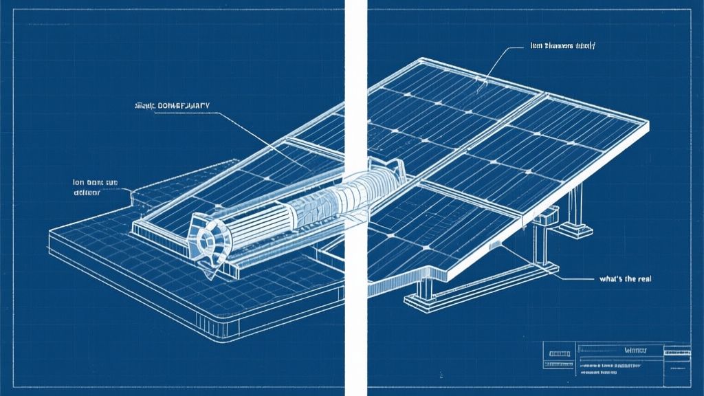
Silicon solar cells just got a quiet upgrade. Researchers at the Indian Institute of Technology Bombay used ion beam implantation to precisely dope silicon with boron, slashing defects that sabotage charge transport. The result? More efficient and reproducible p–n junctions—the heart of every solar panel—without the variability that plagues traditional doping methods. PV Magazine reports the technique could push photovoltaic performance past current limits, but the real test is whether labs can translate this precision into factory floors.
For manufacturers, the promise is tantalizing: fewer defects mean higher yields and lower costs per watt. Yet ion beam systems aren’t cheap, and retrofitting production lines isn’t trivial. The study’s authors suggest the method could be a scalable alternative to thermal diffusion, but NREL’s roadmap notes that scalability often stumbles on throughput—not just precision. Early adopters like 1366 Technologies (now part of Hanwha) have tried similar approaches, only to find that speed and cost still dictate what gets commercialized.
The user reality? If this sticks, homeowners won’t see flashy new panels—just slightly better efficiency in the same form factor. That’s the incremental progress that actually moves markets, not the breakthroughs that never leave the lab.

The workflow shift hiding behind cleaner p–n junctions📷 Source: Web
The workflow shift hiding behind cleaner p–n junctions
Where this gets interesting is in the supply chain. Silicon wafer producers like Longi and JinkoSolar are locked in a race to shave pennies off per-watt costs. Ion beam doping could give them an edge, but only if the equipment vendors—companies like Varian or Axcelis—can deliver systems that don’t bottleneck production. The technology’s precision is undeniable, but solar manufacturing is a volume game, and every extra second in the doping process adds up.
There’s also the question of what this means for next-gen materials. Perovskite-silicon tandems are the darling of R&D right now, but if ion beam doping can push pure silicon closer to its theoretical efficiency limit (~29%), it might delay the shift to more exotic (and unstable) alternatives. That’s a win for reliability, but a headache for startups betting on perovskites to disrupt the market.
The ecosystem effects ripple further. If ion beam doping becomes standard, it could reduce reliance on toxic chemicals used in traditional doping processes—a regulatory win. But it also raises the bar for smaller manufacturers who can’t afford the capital expenditure. The solar industry has always been a balance of innovation and pragmatism, and this is no exception.
For manufacturers, the choice is stark: invest in precision now and hope the cost curve bends, or double down on volume and risk falling behind. For consumers, it’s simpler—better panels at the same price, or slightly cheaper ones with the same performance. Either way, the winners will be the companies that treat this as a manufacturing challenge, not a scientific one.